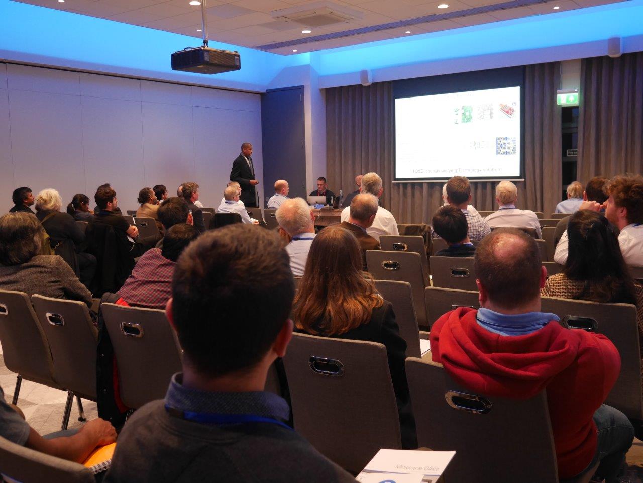
Young Engineer Sponsorship: The ARMMS RF & Microwave Society provides sponsorship for young engineers (28 or below) who have had papers accepted for presentation at each meeting. Abdul Moiz Ahmed of The University of Manchester and Dipendra Mistry of Phasor Solutions were sponsored to attend the November 2018 meeting. Sponsorship is £100 cash plus free attendance (including conference dinner and overnight accommodation). This will be increased to £200 from April 2019. Potential candidates should identify themselves as eligible at time of submission and state their date of birth. This offer is limited to a maximum of 2 places per meeting.
Best Paper Award: The Steve Evans-Pughe prize is awarded to the best presenter at each meeting. Sidina Wane of eV Technologies won the November 2019 award, the runner-up was Dipendra Mistry of Phasor Solutions. The award is £200 for the best paper and £50 for the runner-up. The prize is sponsored by NI.
For exhibition enquiries please email exhibition@armms.org, for all other enquiries please email enquiries@armms.org
 |  |  |
Wyboston Lakes
Great North Road
Wyboston
Bedfordshire
MK44 3AL
| Web | http://www.wybostonlakes.co.uk/ |
David Morris
Keysight
24GHz FMCW Radar With Virtual Antenna. Basic Theory and Real-World Measurements | |
| Mike Roberts | |
| Slipstream Design | |
As millimetrewave radar continues to be used more and more in our every day lives, this paper reviews the principles behind FMCW radar, RF hardware and associated 2D FFT doppler, range and angle processing. We take a look at how virtual antenna are formed by precise physical layout and additional processing. A 24GHz evaluation radar from Analog Devices is used to take measurements of various real-world targets with synchronised video to show the target scene. A plated 3D printed corner reflector is also used to generate a target of known area to provide practical evaluation of achievable range resolution. | |
| 24GHz FMCW Radar With Virtual Antenna. Basic Theory and Real-World Measurements | |
An SMT Packaged 4-Channel mm-Wave PA for 5G Applications | |
| Mohammed Tahir, Stuart Glynn, Liam Devlin, Andy Dearn, Graham Pearson | |
| Plextek RFI | |
5G mobile devices operating at mmWave will incorporate electronic beam steering to address the difficulties of non-line of sight communications at these high frequencies. This requires the use of multiple parallel receive and transmit channels, which must be implemented in a low cost, compact manner. This presentation will describe a 4-channel PA covering the 27.5 to 28.35GHz 5G band designed by PRFI. It was realised as a single chip component on the 0.15µm E-mode GaAs PHEMT process of Sanan IC and is packaged in a standard over-moulded, 5mm x 5mm plastic QFN package. This results in a low cost, SMT compatible component suitable for incorporation into high volume commercial products. Each PA exhibits a gain of 20dB with an RF output power of 24.5dBm at 1dB gain compression with a PAE of 20%. When operated at 7dB back-off to preserve modulation fidelity the third order intercept point is 31dBm | |
| An SMT Packaged 4-Channel mm-Wave PA for 5G Applications | |
Artificial Intelligence design of microwave antennas with case studies | |
| Moyablode Olusola Akinsolu | |
| Gwyndwr University | |
With the advent of artificial intelligence (AI), the design of microwave devices such as antennas has been expedited in terms of throughput and time-to-market. This is chiefly because design automation via optimization has replaced the use of time intensive manual design techniques which premise on trial and error without any guarantee of successful outcomes. For the rapid design of antennas via optimization, surrogate model-based optimization (SMBO) methods tend to be at the forefront due to their efficiency improvement in terms of computational cost. | |
| Artificial Intelligence design of microwave antennas with case studies | |
Broadband matching of continuum mode Power Amplifiers using Particle Swarm Optimisation | |
| Nagaditya Poluri and M. M. De Souza | |
| The University of Sheffield | |
Even though continuum modes such as class B/J continuum, CCF and CCF-1 offer a large choice of impedances in the design of an amplifier, only those which satisfy the Foster reactance theorem can be utilized in practise. The a priori selection of these impedances has been shown to minimize the search space for the amplifier design, thereby resulting in the simplified amplifier design process [1]. This procedure has been demonstrated for the design of Class B/J continuum and CCF, however, a generic procedure to find the impedances does not exit. In a typical amplifier design methodology, the step to find the matching network of selected impedances, often requires trial and error of several topologies thatmay be avoided by the use of the Real Frequency Techniques. In this work, we combine the steps for selection of impedances and matching network to demonstrate a methodology which finds the optimal impedances in the design space of continuum mode as well as the corresponding ideal matching network of RFPAs simultaneously. | |
| Broadband matching of continuum mode Power Amplifiers using Particle Swarm Optimisation | |
Calibration techniques for on-wafer S-parameter measurements | |
| Xiaobang Shang and Jian Ding | |
| NPL and Filtronic | |
Accurate characterisation of S-parameters (scattering parameters) at chip level is of great importance to the development of next generation electronic devices. Such measurements are usually carried out on a Vector Network Analyzer (VNA), subject to an on-wafer calibration. Calibration techniques play a key role in determining the accuracy of on-wafer measurements. This presentation is intended to provide an overview of conventional calibration techniques, including TRL (Thru, Reflect, Line), Multi-Line TRL, and SOLT (Short, Open, Load, Thru), etc. New SOLT calibration method (using a 10-term error model), developed by NPL, will also be reported. Advantages and limitations of these different calibration techniques will be discussed and summarised. Additionally, this presentation will give an insight into other important factors, related to on-wafer measurements at millimetre-wave frequencies. These factors include design of calibration standards, repeatability of on-wafer measurements, impact from testing environment, etc. | |
| Calibration techniques for on-wafer S-parameter measurements | |
Cognitive Beamformer Chips with Smart-Antennas for 5G and Beyond: Holistic FDSOI Technology Solutions including ASIC Correlators | |
| Sidina Wane et al | |
| eV Technologies | |
This paper presents RFIC MIMO modules integrating beamformer chips (including PAs, LNAs, T/R switches, power combiners/dividers and digital controls) and smart-antenna arrays including down-converters for 5G. Several solutions: 2x2 (16 antennas) and 4x4 (64 antennas) arrays of RFIC beamformer chips are designed, fabricated and experimentally characterized. Wireless 5G links with real-time high data rate video-streaming capabilities are demonstrated using integrated cameras. Field-Field correlation-based over-the-air near-field and far-field test solutions with and without down-conversion are proposed for MIMO/Massive-MIMO phased-array systems both in frequency and time domains. Cognitive BIST solutions are combined with co-array signal-processing. Perspectives for holistic RFSOI technology solutions, including RF-analog-to-digital converters (RF-ADCs) and adaptive body-biasing systems, are drawn in comparison with BiCMOS, GaAs and GaN based technologies. | |
| Cognitive Beamformer Chips with Smart-Antennas for 5G and Beyond: Holistic FDSOI Technology Solutions including ASIC Correlators | |
Development of a Spherical Near Field Measurement System for Phased Array Antenna?s | |
| Dipendra Mistry | |
| Phasor Solutions | |
Near-Field measurement of antennas has gained popularity over the last few decades. This is due to its ability to provide excellent measurement accuracy in controlled lab conditions, without the complexities of testing in an outdoor range. A common application for this technique is the calibration and measurement of phased array antennas in the far-field. After array calibration the phased array antenna will beam-form a radiation pattern in the desired given direction across a range of operating conditions. | |
| Development of a Spherical Near Field Measurement System for Phased Array Antenna?s | |
Development of an Analogue Phased Array Beamformer for Wide Ku/K Band Applications | |
| Ben Kieniewicz | |
| European Engineering and Consultancy Ltd | |
This paper presents the design and measurement of a wide 16-22 GHz scalable multi-beam phased array analogue beam former. As the current trend of new chipsets which contain ever more RF circuitry continues, the techniques and principles required to use them also become more challenging. This paper looks at the design criteria required to pack huge amounts of RF circuits together and ensure compliance to beam former theory. The use of automated test and measurement is discussed and how the calibration challenges of such a system can be overcome. The paper uses results and experience which came from the development of EECLs scalable multi-beam, 16/64/256 antenna array. | |
| Development of an Analogue Phased Array Beamformer for Wide Ku/K Band Applications | |
Direct S-Band Communication Using Xilinx's RFSoC and Design-In of its Microwave Interfaces | |
| Rajan Bedi | |
| SpaceChips | |
"Xilinx's RFSoC is a single-chip solution combining RF ADCs and DACs with a 16 nm, Zynq UltraScale+ MPSoC capable of implementing a complete software-defined radio including direct IF/RF sampling at the receiver and direct IF/RF re-construction at the transmitter. 12-bit, 4 GHz ADCs are available capable of sampling up to 2.058/4 GSPS allowing direct digitisation of UHF, L and S-band carriers within this input bandwidth, as well as 14-bit, 4 GHz DACs sampling up to 6.554 GSPS allowing reconstruction of IF/RF signals and direct up-conversion to the second Nyquist zone within this output bandwidth. Portable, ground terminals for satellite communication and M2M applications are baselining RFSoC because it offers the potential to produce small, low-power, highly-integrated transceivers. Many companies struggle with designing the analogue, microwave interfaces before and after theRF ADCs and DACs respectively. Broadband impedance matching, passive or active, single-ended or differential circuitry before and after the mixed-signal convertors, as well as RF simulation and synthesis, are key challenges for today's digital-centric engineers." | |
| Direct S-Band Communication Using Xilinx's RFSoC and Design-In of its Microwave Interfaces | |
High Efficiency Class E MMIC Oscillator for X-Band Medical Applications- part A | |
| Abdul Moiz Ahmed Pirkani, Christopher I Duff, Robin Sloan | |
| The University of Manchester | |
RF and microwave devices have effectively found applications in the field of medicine and electrosurgery due to the non-ionizing nature of RF and microwave energy. Microwave power sources can be combined with suitably designed antenna and applicator structures to produce highly focused and controlled heating on tissue structures; while minimising distributed tissue heating and the effect on neighbouring tissues [1]. This is called Microwave Ablation. Electrosurgical devices operating at C-band and X-band Presented herein is a high efficiency class E oscillator targeted for X-band and Ku-band surgical devices for the treatment of: tumours, gastro oesophageal reflux disorder, and spider veins. The oscillator has been developed using 4x150 μm GaAs pHEMT transistor Presented herein is a high efficiency class E oscillator targeted for X-band and Ku-band surgical devices for the treatment of: tumours, gastro oesophageal reflux disorder, and spider veins. The oscillator has been developed using 4x150 μm GaAs pHEMT transistor from the WIN PP10-15 MMIC process with support from Semtech Limited. Design, EM simulations and layout have been performed in Keysight’s ADS following a three step design procedure 1) Design of class E switching mode amplifier for optimised PAE performance 2) Design of appropriate feedback network according to the terminal voltages and currents 3) Transient analysis and large-signal optimisation of the oscillator The design of class E amplifier involves selection of: optimum load impedance at the fundamental frequency (also the frequency of oscillation) through load pull analysis, and conjugately matched source impedance to drive the transistor in saturation region. Once the amplifier has been optimised for high power and PAE through large signal EM simulations; voltages and currents at the amplifier’s input and output reference planes are obtained. These are then used to design the feedback network required to provide start-up conditions for the oscillations. In the third step, transient analysis is performed and the oscillator is optimised at the design frequency for the required power and efficiency. | |
| High Efficiency Class E MMIC Oscillator for X-Band Medical Applications- part A | |
Microwave S-parameter calibration techniques and their uncertainty | |
| Dilbagh Singh, M Salter, N Ridler | |
| NPL | |
This paper discusses techniques for calibrating vector S-parameter network analysers and uncertainties associated with the measurements due to the calibration techniques. The paper discusses different calibration methods and their typical applications and then a number of devices are measured using the same equipment, calibrated with different methods and the measured results are presented. The investigation has been carried out over 100 MHz and 26 GHz, which covers many of today’s RF/Microwave applications. Six different types of calibrations have been investigated on a number of one-port and two-port devices. The measured uncertainty is also compared to the UK’s Primary Impedance Microwave Measurement System. | |
| Microwave S-parameter calibration techniques and their uncertainty | |
Multi-port Amplifier fed Linear Array | |
| Peter James | |
| Airbus | |
The object of this paper is to describe the possibility of feeding a linear array with a pair of MPAs, so that a variable amplitude taper can be applied to the array. This may be achieved by switching edge elements off completely or giving them relatively low amplitude, whilst at the same time using all the amplifiers at or near their maximum. Hence the array may be used most efficiently. The aim of this paper is to show that a pair of 8x8 MPAs may feed a linear array. It will also present some predictions of the radiation patterns. | |
| Multi-port Amplifier fed Linear Array | |
Provision of UK GaN MMIC capability for X-band applications | |
| Dr Jacek Gryglewicz | |
| INEX | |
Future systems in space, defence and commercial markets will rely heavily on beam-steering array systems to provide high performance connectivity. Presently, designers are engaged in developing single-chip solutions for largescale antenna systems. The optimum technical solution is a single-chip gallium nitride (GaN) front-end driven by either a gallium arsenide or silicon-germanium driver chip. However, many defence subcontractors and design teams have highlighted the need for a sovereign capability as existing GaN foundries are located around the world each suffering from various IP, competition and export issues. INEX Microtechnology Ltd. (INEX) has developed a sovereign GaN technology supply chain to mitigate many of the barriers to new markets and ensure secure supply. The first offering is IG50 a process focussed on delivering performance up to, and including, X-band. The paper will discuss the key challenges in the technology development and present performance metrics at X-band. It will also introduce the process design kit released for Keysight’s ADS. | |
| Provision of UK GaN MMIC capability for X-band applications | |
Your recipe of on-wafer calibration for accurate mm-wave characterisation of advanced silicon devices | |
| Andrej Rumiantsev | |
| MPI Corporation | |
System calibration is irreplaceable step of the RF device characterisation process. Traditionally, it consists of two tiers: the first is the probe tip calibration performed on a commercially available coplanar calibration substrates. The second-tier is the de-embedding of the device infrastructure parasitic. Is is conducted using a set of wafer-embedded device-specific de-embedding elements, aka de-embedding “dummies”. We will demonstrate that the characterisation of advanced silicon devices requires alternative approach. We will discuss solutions for both metrology-grade and production-suitable calibration methods and will share some experimental results and practical recommendations. | |
Companies booking two or more delegate places are able to take part in the commercial exhibition that accompanies the conference. Please note: there is a maximum of 20 exhibition tables at each meeting, these are offered on a first come basis. Booking two delegate places does not guarantee an exhibition space, please email exhibition@armms.org to check availability and reserve and exhibition space.
The society would like to thank RFMW and Qorvo for sponsoring the November 2019 meeting:
Contributions are invited with an emphasis on RF and microwave design, research, testing and associated subjects. An oral presentation will be made at the meeting and a written paper will be required for publication in the society digest, which is distributed to delegates at the meeting. Prospective speakers are requested to submit a title and a short abstract to the technical coordinator (see above) as soon as possible.
Click here to view our Guidelines for Authors
Click here to view our Publication Release Form