 |  |  |
Rockingham Forest Hotel
(Formerly Hotel Elizabeth Rockingham)
Rockingham Road
Corby
Northamptonshire
NN17 2AE
| Tel | 01536 401348 |
| Fax | 01536 266383 |
| rockinghamforest@butterflyhotels.co.uk | |
| Web | www.butterflyhotels.co.uk/Our_Hotels/Corby/index.php |
Aaron Tang
QinetiQ
| Tel | 01684 896414 |
| ahtang@taz.QinetiQ.com |
A Compact, Agile, Low-phase Noise Frequency Source with AM, FM and Pulse Modulation Capabilities | |
| Alexander Chenakin | |
| Phasematrix | |
| This paper presents a broadband frequency source featuring high technical characteristics and extended functionality. The source is a compact (5 by 7 by 1 inches) module that covers the 0.1-to-10 GHz frequency range with a 0.001 Hz step size. The module is based on a novel (patent pending) PLL design that combines fast switching speed, low phase noise, and low spurious characteristics. The measured phase noise at an output frequency of 10 GHz and 10 kHz offset is �122 dBc/Hz. For an output frequency of 0.1 GHz and 10 kHz offset the phase noise drops down to �150 dBc/Hz. The switching time is about 20 uSec to be within 1 MHz from the final frequency and less than 100 uSec to be within 50 kHz respectively. Spurs do not exceed the �70 dBc level. The output power is leveled between �25 and +15 dBm. The module can be controlled through either SPI or USB interface and also includes AM, FM and pulse modulation capabilities. The developed module can be used as a broadband, agile, high-fidelity signal source in a variety of test-andmeasurement, communication, and surveillance systems. | |
| A Compact, Agile, Low-phase Noise Frequency Source with AM, FM and Pulse Modulation Capabilities | |
A Low Cost High Power, High Voltage, 150MHz Solid State Amplifier for Pulsed Applications | |
| M. Walden, R Harrison, M. Mills, D. Pennington, P. Wilkinson, A. Cook | |
| Roke Manor Research | |
| Traditionally tube amplifiers still dominate high power applications at VHF frequencies. However a team at Roke are developing a low cost solid state alternative. In this paper we report our initial investigations and the development of the unit cell structure that will be combined to create a modular amplifier. The requirement for low cost led us to using commercially available RF MOSFETs as the basis for our unit cell design. Taking a single device we were able to achieve over 2kW of pulsed output power with a power gain in excess of 15dB. | |
| A Low Cost High Power, High Voltage, 150MHz Solid State Amplifier for Pulsed Applications | |
A Network Application Interface for RCS Calculations | |
| Philip Galloway | |
| Roke Manor Research | |
| This paper describes a Network Application Interface, Network (API) that has been added to the EpsilonTM Radar Cross Section (RCS) Predictions Code. EpsilonTM is a well established Physical Optics (PO) based prediction code with Shooting Bouncing Ray (SBR) multiple scattering and Physcial Theory of Diffraction (PTD) edge scattering facilities. The Network API is a recent addition to the product that allows users to utilise the RCS prediction engine into their own applications. The main use of this facility is anticipated to be for the incorporation of accurate RCS data into simulation frameworks. We describe the Network API, and provide an example of how the API has been used within a simulation of a Multi-Static Passive Radar(MSPR) system. | |
| A Network Application Interface for RCS Calculations | |
An Integrated 3DEM Design Flow for the Design of High Performance RF Electronic Devices | |
| Saliou Dieye | |
| Agilent | |
| As our electronic appliance world becomes increasingly small, and compact, wireless electronic component vendors compete to squeeze more RF functionality into ever smaller packages at lower costs to capture the high-volume consumer market. This is cost pressure has driven the emergence of innovative interconnection and packaging technologies. One of the enabling technologies is RF-system in package (SiP). It includes multiple bare IC dies, embedded passive, and SMT components integrated into a small package and designed to perform multiple functions. In RF SiP components, bond wire interconnections are often used to connect the IC dies together. Today, designers are trying to shrink the components size with newer interconnection technologies such as TSV (Through Silicon Via). EM (electromagnetic) interferences, radiation effects, and unwanted coupling between devices are one of the highest design challenges. If not contained, they can jeopardize the functionality of a complete system. This implies circuit re-spin, lengthening product development time, and development cost increase. This presentation introduces the audience to an integrated high frequency design flow. It relies on a high performance RF simulator tightly integrated with the state of the art EM solvers to quickly identify and mitigate the negative impact of electromagnetic interferences. | |
| An Integrated 3DEM Design Flow for the Design of High Performance RF Electronic Devices | |
C-band High Speed Downlink for LEO Satellite | |
| Colin McLaren | |
| Comdev, UK | |
| For small satellite applications where spacecraft bus power is very limited the efficiency of the high power devices on board is critical. Amongst these are the downlink transmitters which, although they only operate for a small percentage of the orbit (typically around 10%), do consume relatively high levels of power for this period. This paper presents a high efficiency 5W C Band Transmitter for small satellite applications built around a GaN based Class AB power amplifier. The Transmitter accepts input data at a rate of 20Mbit/s and the baseband processing applies scrambling, FEC and pulse shaping. This is mapped to a pair of I & Q signals that are applied to a direct vector modulator. The analogue baseband can be either QPSK or OQPSK. The vector modulator translates the baseband directly to 5.2GHz and is routed to the power amplifier followed by a lowpass filter (LPF) to allow the out-of-band rejection requirements to be met for the entire sub-system. | |
GaN technologies: Applications, status and trends | |
| Didier Floriot | |
| UMS | |
| GaN technology has gained a lot of attention in Europe over the last few years for various domains including RF electronics. This presentation will try to present a brief summary and the current status achieved of the GaN technology in Europe in comparison to the competition around the world. Due to the importance of the subject this paper will focus solely on the RF electronics related topics. Aspects covering material, devices up to circuits and module integration will be addressed. Thanks to many partnerships in Europe with National Research Institutes, UMS has pushed the development of GaN technologies in order to be at the end the leading company in Europe on this topic. Two technologies associated to gate length of 0.5�m and 0.25�m have been identified covering respectively application needs up to 7 GHz (transistors and power bars) and MMICs up to 20 GHz. These technologies will cover the full spectrum of telecom, defence and space applications. State of the art results will be shown from L to C bands on elementary power transistors and power bars (Radar, telecom) and preliminary results in X-Band and Wideband applications for Radar and EW applications. Some elements of reliability will be also given, summarizing the current status and key challenges on which progress is expected. | |
| GaN technologies: Applications, status and trends | |
High Stability Microcontroller Compensated Crystal Oscillator | |
| Damien Camut | |
| Europa Electronics | |
| Microcontroller Compensated Crystal Oscillators (MCXO) are described which use an ARM type processor embedded in field programmable grid array (FPGA). Crystal oscillators are used for frequency generation due to very good stability capability. The main instability contributor is the temperature variation. Two main technologies are employed: manage the temperature environment of the crystal resonator or compensate for the effect of temperature on the crystal resonators. The first technique is widely used in Oven Controlled Crystal oscillator (OCXO). Compensation techniques are well known through analog Temperature compensated crystal oscillator (TCXO), digital temperature compensated crystal oscillator (DTCXO) and MCXO. This document will describe the technology for high end MCXO. | |
| High Stability Microcontroller Compensated Crystal Oscillator | |
Low Cost Production Phase Noise Measurements on Microwave and Millimeter Wave Frequency Sources | |
| Hugh McPherson | |
| Spectral Line System Ltd | |
| Production test on all high frequency sub-systems is most efficiently carried out using dedicated test benches which once set up and calibrated remain undisturbed for the duration of the contract. In the case of phase noise measurements this can prove expensive if several jobs are running in parallel through production. This paper describes a low cost solution which is particularly suitable to phase noise measurements on microwave and millimetre wave sources, namely the Two-Source IF Discriminator Method. | |
| Low Cost Production Phase Noise Measurements on Microwave and Millimeter Wave Frequency Sources | |
Means of Power Handling Improvements in Ferrite Switches for Space Applications | |
| Imtiaz Khairuddin, Abdullah Abuelmaatti, Colin Mclaren | |
| Comdev, UK | |
| The challenges associated with the ultra fast waveguide ferrite switches for future earth exploring radar instruments are huge in terms of meeting the customer’s aggressive requirement of size, low insertion loss and high power handling (>600W CW). Traditionally, four ports having two 90o ferrite phase shifters, waveguide magic TEE and a waveguide 90 degree hybrid configured in a variable power divider are used as a two-way switch for such high power applications. But, such switches are larger in size and possesses slower switching speed Where, the compact sized Wye shaped resonators based switches operating in a high order TM mode can, with careful design, handle up to >100W in X to K frequency bands. The main hurdle to improving the average power is the relatively large area of the ferrite Wye that is not in contact with any heat sink and hence suffers larger temperature extremes and gradients. In this method rectangular blocks of low dielectric constant with relatively good thermal conductivity are used as heat sink to provide additional thermal paths from ferrite Wye resonator (which itself has rather poor thermal conductivity) to the waveguide housing leading to an improvement in the average power handling. The paper presents detailed comparisons of both approaches described above and in particular compares the expected performances, using the standard Wye design as a baseline, in terms of power handling, size, insertion loss, isolation, switching speed and the frequency bandwidth. | |
Millimeter Wave Integrated Array Antenna | |
| Greg Ball | |
| QinetiQ | |
| This presentation will describe the design, fabrication and assessment through measurement, of a small millimetre-wave horn antenna, a candidate element for a focal plane array. The design was undertaken using commercial electromagnetic software and the fabrication was achieved using micro-machining techniques. The design process and the fabrication will be summarised and discussed. Results from the measurements, including return loss and gain versus frequency together with radiation patterns, will be presented and compared with predictions. | |
Nonlinear Behavioral Models, Measurement Systems and their use in Circuit Simulators | |
| Malcolm Edwards | |
| AWR | |
| To-date the vast majority of RF and Microwave designs have been developed by using either discrete device models or S parameters. These two approaches to modeling have served as the circuit descriptions of active devices and subsystems. S Parameter data can be rapidly acquired and deployed, but are limited to describing the linear processes only. Alternatively; robust and accurate discrete device and subsystem models has always presented significant challenges - sophisticated measurement, parameter extraction, model testing and delivery of model parameters to the end user in a timely fashion. With the advent of more complex behavioral models such as the Cardiff Model, X Parameters and S Functions and their closely linked measurement systems, designers can now generate data driven models that describe the nonlinear behavior of their components in near to real time. These new approaches to modeling avoid the limitation of S Parameter models applying to linear systems only and the complexity of discrete device model generation. This paper describes some of the background to these new and exciting approaches to device and subsystem modeling. | |
Recent and Future Developments in Millimetre and Sub-millimetre Wavelength Measurement Standards at NPL | |
| David B. Adamson, John Howes, Nick M. Ridler | |
| National Physical Laboratory, UK | |
| With the rapidly growing interest in millimetre-wave and sub-millimetre-wave systems, the lack of traceability for measurements at these wavelengths is becoming ever more of a problem. Making comparable measurements of fundamental parameters, such as power, is very difficult and no proper calibrations traceable to SI realisations are available. At NPL, work undertaken in the 1980s led to the development of the photo-acoustic power meter by QMC, London (now marketed commercially by Thomas Keating) but this does not easily address measurements of power in waveguide. NPL also has comprehensive standards (power, S-parameters, noise and attenuation) in waveguide up to 110 GHz but nothing (until recently) at higher frequencies. This paper gives a brief overview of existing work above 110 GHz, recent work up to 110 GHz which serves as a foundation for extension above 110 GHz and future plans for work up to 500 GHz. | |
| Recent and Future Developments in Millimetre and Sub-millimetre Wavelength Measurement Standards at NPL | |
Schottky Diode Technology at the Rutherford Appleton Laboratory | |
| Byron Alderman | |
| STFC Rutherford Appleton Laboratory | |
| Most parts of the electromagnetic spectrum are well understood and exploited, but the terahertz region between the microwave and infrared is still relatively under developed. Potential receiver applications are wide-ranging and cross-disciplinary, spanning the physical, biological, and medical sciences. In this spectral region, Schottky diode technology is uniquely important. InP MMIC amplifiers are generally limited to frequencies less than ~200 GHz, above which their noise performance rapidly deteriorates. Superconducting circuits, which require cooling, may not always be practical. Either as varistor diodes (heterodyne mixing), or varactor diodes (sub-millimetre power generation), Schottky technology underpins terahertz receiver development. Two important developments have occurred in recent years. First, the underpinning technology base has demonstrably matured. Planar Schottky diode technology has been shown to be practical at frequencies as high as 2,500 GHz, and frequency multipliers have been shown to be capable of generating 100's of mW at frequencies around W-band. Secondly, circuit designs can now be optimised theoretically with CAD electromagnetic structure simulators and non-linear analysis programs. New high-speed computer controlled mills, improved lithographic capabilities and micro-machining techniques also offer exciting new options for cavity and circuit manufacture. This paper describes the Schottky diode technology currently being developed at the Rutherford Appleton Laboratory. Discrete diode components are described as well as integrated diode/filter circuits. Mixer and multiplier diode structures are reported which include novel substrate transfer techniques to reduce the effects of dielectric loading and self-heating. | |
| Schottky Diode Technology at the Rutherford Appleton Laboratory | |
Structured Surface on Subwavelength Controllable Surface Plasmon | |
| Zhirun Hu, Adnan Noor | |
| University of Manchester | |
| The demand for broadband and thin layer radar low visible surface for use in future defence systems has been a great challenge. Although the existing technology has already achieved low RCS, a step improvement in the performance will be needed for future systems. The current techniques to reduce RCS are mainly based on shaping the surface, absorbing the incident wave and scattering. By properly designing the shape of a surface, one can reduce the specular reflection significantly, hence very low monostatic RCS. However, this technique can�t reduce bistatic RCS, which makes the object easily detectable for more sophisticated radar networks. While radar absorbers/scatters can well be implemented on ground/sea objects, broadband and thin layer absorbers/scatters on flying objects still remain very challenging. There has been a great interest on cloaking an object, or in other word, making an object invisible. There are basically two approaches to cloak an object: coordinate transformation and cancellation of scattering fields of the target. While the former approach might work on a reasonably wide bandwidth, at least, in theory, it is still a distance away from practical applications. The latter works based on the idea that the field generated by an object can be decomposed into spatial harmonics. The lowest order spatial harmonic of the target is then cancelled out by that of the cloak. However this approach can only be applied to sub-wavelength targets at fundamental polarisation direction. In addition the cloak only works for certain shapes. Recently, it has been proved, both theoretically and experimentally, that it is possible to control the interaction between incident electromagnetic wave and structured metal surface to give rise to so called spoof Surface Plasmon Polaritons (spoof SPPs). Unlike classic SPPs on unstructured metal surface, spoof SPP dispersion and spatial confinement of the surface bound modes can be engineered at will. This opens a new avenue for confining and manipulating electromagnetic wave at shallow surface by creating spoof surface plasmonic modes with desired dispersion through structure design. Since the spoof surface plasmonic modes can be induced as long as the structured surface with subwavelength unit cells and exist as evanescent waves at air-metal interface, one can envisage that such structured surface can be very thin and operate at very wide bandwidth. We will review the progress in the field and works carried in the University of Manchester. | |
| Structured Surface on Subwavelength Controllable Surface Plasmon | |
The Design Challenges of RF SiPs and Multi Chip Modules | |
| Andrew Wallace | |
| Applied Wave Research Ltd | |
| With the design constraint of increasing component count coupled with the challenge of managing high speed digital and microwave signals RF Modules and SiPs designers require a sophisticated selection of design tools. These design challenges are addressed by EDA vendors in providing design frameworks which provide a seamless interface to a comprehensive set of synthesis, simulation and verification solutions. The old working methodologies of using a weakly bound set of point tools linked together with an ad hoc and poor data transfer mechanism are dying fast. By combining the optimum technologies for each function the system performance can be maximized: for example CMOS for digital; GaAs or SiGe for RF Microwave processing along with soft-board laminates and LTCC for packaging and interconnect. In essence, this mix of technologies is the basis of the definition of an RF Multi Chip Module or System in Package. This paper will discuss tool and design flow concepts of RF Modules from the perspective of design entry and simulation. | |
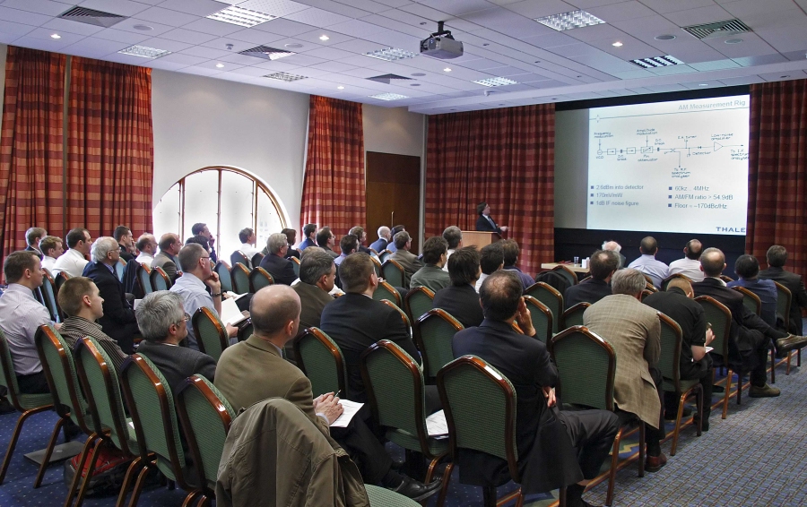
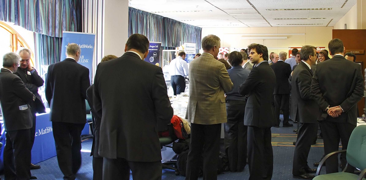
As usual there was an accompanying exhibition. Companies wishing to exhibit at future meetings should email: exhibition@armms.org
Contributions are invited with an emphasis on RF and microwave design, research, testing and associated subjects. An oral presentation will be made at the meeting and a written paper will be required for publication in the society digest, which is distributed to delegates at the meeting. Prospective speakers are requested to submit a title and a short abstract to the technical coordinator (see above) as soon as possible.
Click here to view our Guidelines for Authors
Click here to view our Publication Release Form